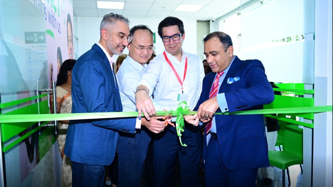
Synopsys Opens new Chip Design Centre at DLF Tech Park in Noida
#Synopsys #ChipDesign #DesigninIndia #SemiconductorchipsThe new chip design centre is testament to the growing ecosystem of fabless chip design and innovation in India.
Jan 2024 : Rajeev Chandrasekhar, Union Minister of State for Electronics and IT, Skill Development and Entrepreneurship, and Jal Shakti, is set to inaugurate Synopsys’ Chip Design Centre at DLF Tech Park in Noida on Jan 23, 2024.
Established in 1986, Synopsys widely commercialized logic synthesis, revolutionizing the creation of digital designs from language descriptions. This capability propelled the transition of Computer-Aided Design (CAD) into the Electronic Design Automation (EDA) era, facilitating the scaling of digital complexity in line with Moore’s Law. Today, Synopsys is a leading name in EDA, playing a pivotal role in advancing digital chips within the technology ecosystem.
It offers a wide range of design portfolios, spanning from silicon to software, contributing to US$5.9 billion in revenue. The firm has also established the second-largest design center in India. This center is home to approximately 6,000 engineers from India, constituting 27 percent of their global design workforce.
While it’s an established fact that 20 percent of global VLSI/Chip designers are from India, the increasing footprint of Synopsys in Noida, hosting 1650 engineers to begin with, stands as a testament to the growing ecosystem of fabless chip design and innovation in India. Synopsys’ Indian engineers are not only contributing to every aspect of the design cycle of semiconductor chips/IP Cores but are also participating in the success stories of all leading semiconductor companies. Almost all the chips designed by any company use EDA/IP solutions in one way or another.

NEWSLETTER
TRENDING ON PRO MFG

MORE FROM THE SECTION